InPsy's die-to-die IP conforms to the latest UCIe specifications and is a state-of-the-art high speed interface for next-gen multi-die and chiplet architectures

InPsy’s UCIe-A PHY IP delivers the high-speed, low-latency, and energy efficient die-to-die connectivity demanded by next-generation AI, HPC, and datacenter systems. Fully compliant with the UCIe 3.0 standard and backward compatible with the UCIe 2.0 and 1.1 standards, it supports data rates of up to 64 Gbps per lane and offers multiple configurations purpose-built for silicon interposers, silicon bridges, and other TSV-enabled advanced packaging architectures.
Key Features
InPsy’s UCIe-S IP builds on the same core design principles as the UCIe-A family, offering a refined variant tailored for longer-reach, high-density chiplet connectivity over organic substrates, high density substrates, and other lower cost 2D packaging platforms. Fully compliant with the UCIe 3.0 specification and backward compatible with the UCIe 2.0 and 1.1 standards, the UCIe-S IP delivers optimized lane rates and exceptional energy efficiency for die-to-die links requiring high speed connectivity and low latency. Various configurations of this IP support a broad range of system architectures.
Key Features
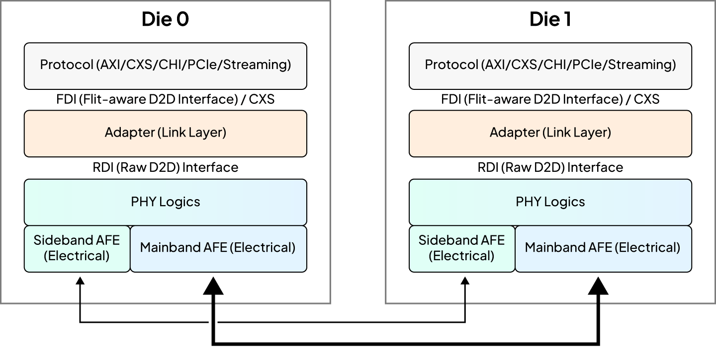
The adapter provides Flexible Data Interface (FDI)–to–Universal Data Interface (UDI) bridging with a low-latency, high-throughput streaming architecture, fully compliant with UCIe 1.1, 2.0, and 3.0. Its flexible, standards-aligned design ensures interoperability with other UCIe IP for seamless integration in next-generation chiplet systems.
Key Features
Designed for maximum interoperability, the UCIe protocol layer supports AXI, CHI, and PCIe protocol transportation, enabling smooth integration with leading on-chip interconnects and external host interfaces. This multi-protocol support accelerates chiplet adoption by providing a ready-to-use, standards-based solution for next-generation heterogeneous systems.
Key Features
InPsy’s UCIe IP Evaluation Kit delivers a fully packaged environment that allows customers to thoroughly explore and validate our UCIe PHY, Adapter, and Controller solutions. Featuring simulation models, reference designs, configuration presets, and guided integration documentation, the kit accelerates the evaluation process and reduces technical uncertainty. It empowers teams to analyze performance, confirm interoperability, and seamlessly assess UCIe technology within their own system architecture - enabling smoother adoption
Key Features

InPsy’s ONFI 3600 MT/s IP is a silicon-proven and widely validated NAND interface that meets the ONFI 5.1 specification. This IP is optimized with focus on tighter electrical, timing, and signal-integrity. It incorporates refined equalization, robust training algorithms, and resilient PVT-tracking to ensure stable high-speed operation. This is a deployment-ready option for SSD controllers, embedded storage subsystems, and other high-performance storage silicon and its proven track record offers predictable interoperability with a broad ecosystem of NAND devices.
Key Features
InPsy’s ONFI 4800 IP is a next gen NAND interface architected with a forward-looking design philosophy that anticipates the key soon-to-be finalized ONFI 5.x specifications. The IP is ground-up engineered with the electrical, timing, and architectural requirements for next gen ONFI 5.x data-rate operation, tighter signal integrity expectations, enhanced command/address structures, and improved reliability features. It delivers a robust and future-proof solution to seamlessly transition to next-generation Flash devices when the 5.x standard is finalized. The ONFI 4800 IP has been validated in successful customer tape-outs, a real-world track record of low integration risk, and consistent interoperability across a range of NAND memory.
Key Features
InPsy’s ONFI 6400 MT/s IP is engineered as the next step beyond the ONFI 5.x generation. This IP anticipates a market with even higher storage and memory bandwidth requirements, driven by AI training and large-scale inference. It also establishes a forward-looking foundation for ultra-high-speed NAND interfaces. The ONFI 6400 enables future-proof designs ahead of the formal standard and the transition to faster ONFI technologies. Built on a resilient high-speed PHY architecture, ONFI 6400 introduces enhanced equalization and new analog front-end capabilities to ensure stable operation at ultra- high data transfer rates. This next-gen interface delivers significantly higher throughput, making it ideal for next-generation SSD controllers and storage-enabling silicon platforms.
Key Features
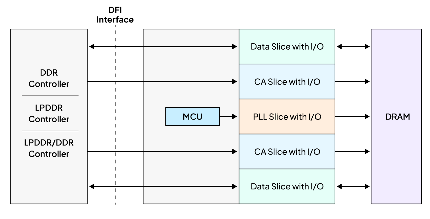
InPsy’s DDR PHY solutions are engineered to deliver exceptional performance, power efficiency, and signal integrity across advanced process nodes, drawing on over 20 years of development and mass-production experience from our founding R&D team - who previously built multiple generations of leading-edge DDR PHY IP on the most advanced-node geometries of their time. Designed to support the demanding performance and timing requirements of modern high-speed DDR interfaces, InPsy’s PHY architectures use optimized transistor structures, multiple Vt device options, and precise drive-strength tuning to deliver strong signal integrity, stable timing margins, and excellent PPA efficiency. The underlying physical design balances density with robustness, ensuring that critical data and command paths maintain consistent performance across wide PVT conditions and at aggressive data rates. Combined with well-engineered I/O structures, reliable on-die termination, and proven calibration techniques, InPsy’s DDR PHY design methodology offers a solid, silicon-proven foundation for customers building next-generation DRAM subsystems with confidence.
Key Features
InPsy’s LPDDR PHY is a cutting-edge, high-performance physical layer interface PHY designed to meet the demanding requirements of modern computing and mobile applications. This PHY supports the latest LPDDR5X standard, providing enhanced data rates, lower latency, and improved power efficiency. It is ideal for applications such as smartphones, tablets, laptops, and high-performance computing systems, where speed and energy efficiency are paramount.
Key Features
InPsy’s DDR and LPDDR Combo PHY supports multiple generations of DDR and LPDDR, providing flexibility, backward compatibility, and supply chain flexibility for HPC, mobile, and data centers applications. It ensures robust performance with high data rates, low latency, and efficient power consumption.
Key Features
This MIPI D-PHY/C-PHY solution adheres to the MIPI Alliance standards and supports scalable link distances, including short-reach, and long-reach modes. It delivers optimized signal integrity and power efficiency for advanced imaging and display pipelines.
Key Features
The custom IO solution includes GPIO, Over-Drive IO (ODIO), fail-safe IO, crystal interfaces IO, high-ESD protection Circuitry, and support for standard IO protocols such as RGMII, eMMC, and ONFI. Can be custom crafted on request.
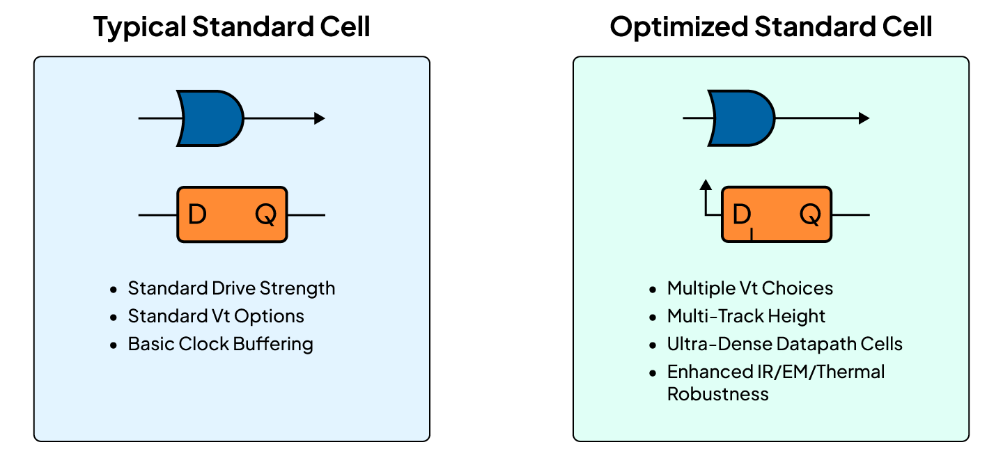
InPsy’s optimized standard cell library delivers exceptional PPA efficiency for customer specific designs on popular process nodes. Variants are purpose-built for high-performance computing, AI workloads, and storage applications. Featuring tuned transistor architectures, multiple Vt options, and refined drive-strength granularity, the library enables higher frequencies, lower latency, and better power control. Available in 6T, 9T, and 12T track-heights.
Key Features
Every product is different and that’s why general-purpose UCIe IP almost always forces uncomfortable PPA tradeoffs - tradeoffs that shouldn’t be necessary given the tens to hundreds of millions of dollars it costs to bring a product to market. InPsy can custom craft the UCIe IP architecture to your exact performance, power, packaging, and reliability targets to avoid these compromises. What’s your priority? Beachfront density, depth, metal-layer or MIM layer reduction, bit-error performance, power efficiency, latency, package type, or unique floorplan constraints? We’ll co-engineer the IP with you to meet your precise specifications without suffering any of the tradeoffs.
Customization services also cover the ONFI IP portfolio. A one-size-fits-all ONFI PHY or I/O macro accumulate limitations as data rates climb, packaging constraints increase, and layout constraints multiply. InPsy’s ONFI customization service tailors the PHY architecture, DQ/DQS timing algorithms, driving strengths, termination options, training sequences, as well as the IOs to your specific NAND configuration and signal-integrity environment. We optimize the IP for your die size, metal stack, energy efficiency, and system-level requirements to deliver an ONFI IP that is cleaner to integrate, features stronger margins, and meets your exact performance targets.
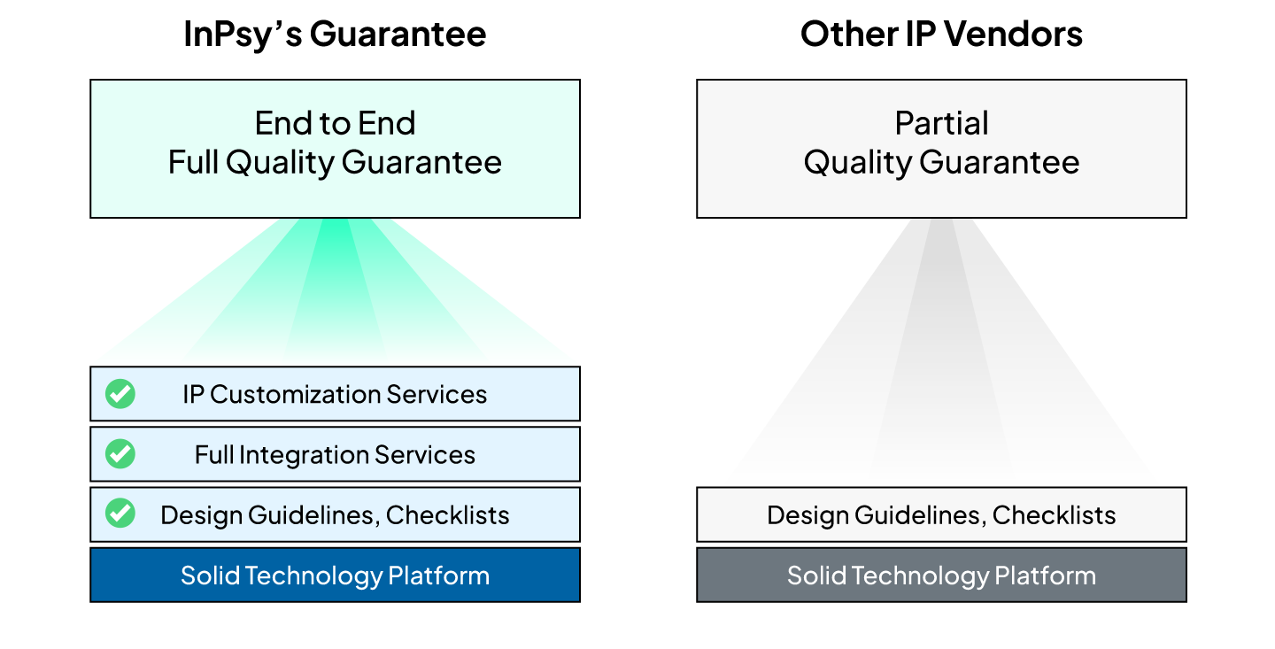
InPsy’s IP Customization Service designs the IP to fit your product - never the other way around.
Key Features
InPsy’s UCIe and ONFI IP Integration Services seamlessly incorporates each IP block into your SoC or chiplet and includes comprehensive cross-domain SI/PI analysis services. We collaborate with your engineering team to deliver smoother bring-up, faster schedules, and first-silicon success.
The UCIe Integration Services co-optimizes PHY placement, beachfront planning, metal-stack usage, timing closure, protocol mapping (AXI, CXS, CHI-C2C, streaming), link-training behavior, SI/PI margin assessments, and 2.5D/3D packaging constraints to guarantee margin-rich and predictable die-to-die performance.
The ONFI Integration Services can tailor the DQ/DQS timing, pad-ring and pin placement, driving strengths, termination schemes, power-grid and IR-drop alignment, and controller-interface so that high-speed NAND interfaces close timing cleanly and operate with robust PVT margins.
Key Features